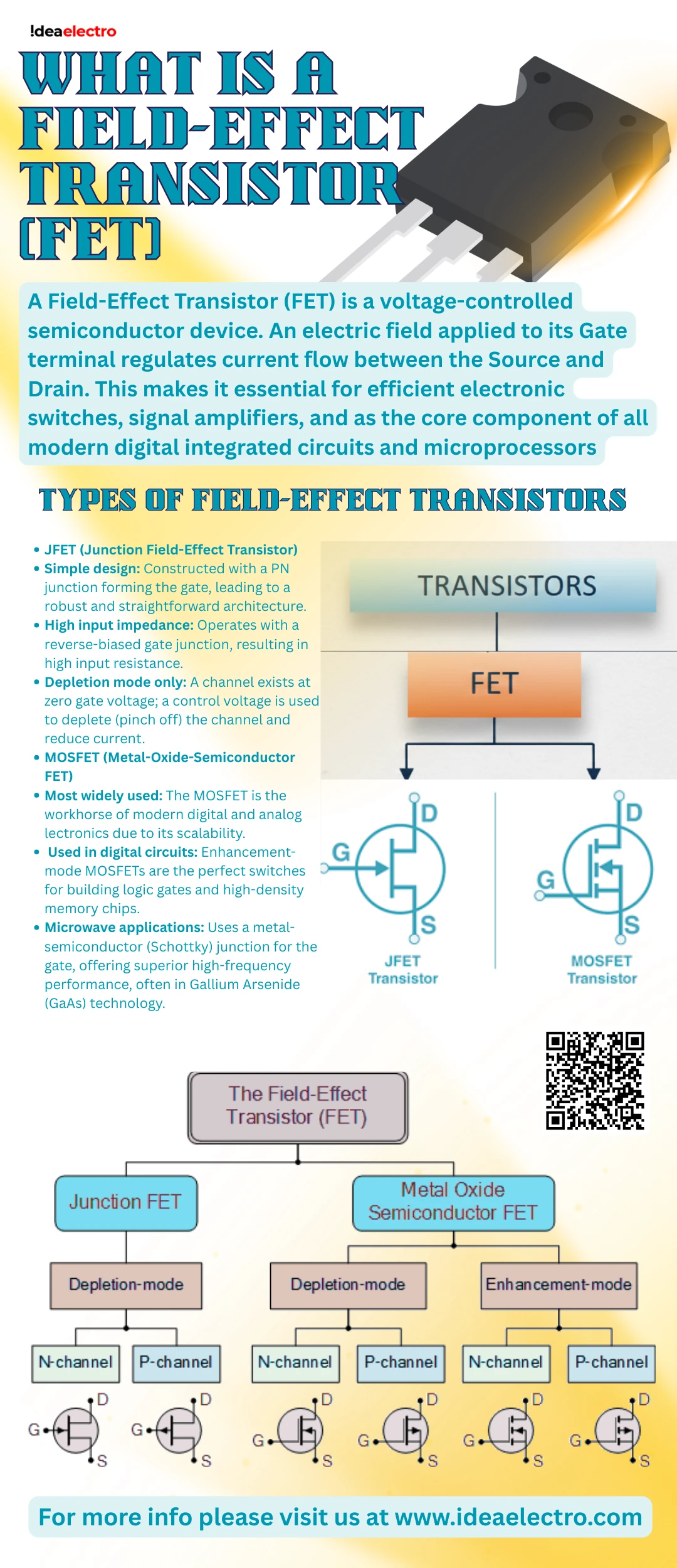
A Field-Effect Transistor (FET) is a foundational semiconductor device that has shaped modern electronics. Unlike its predecessor, the Bipolar Junction Transistor (BJT), the FET is a voltage-controlled device. This means the current flowing through its main channel is regulated by the voltage applied to a control terminal, not by an input current. This core operational difference gives the FET its most celebrated trait: an extremely high input impedance. The high input impedance allows FETs to interface with sensors and other circuit stages without drawing significant current, making them ideal for building efficient and sensitive electronic systems. Their unique properties have made FETs, particularly the Metal-Oxide-Semiconductor FET (MOSFET), the dominant transistor in digital integrated circuits, forming the building blocks of modern microprocessors and memory chips.
- Low power consumptiondue to minimal control current.
- Voltage-controlled operation, simplifying circuit design.
- Widely usedin everything from analog amplifiers to digital computers.
Definition of a Field-Effect Transistor
At its core, a Field-Effect Transistor is a three-terminal, unipolar semiconductor device. “Unipolar” indicates that electrical conduction is facilitated by only one type of charge carrier—either electrons or holes—within the active channel. The primary function of an FET is to use an electric field, generated by a voltage applied to its control terminal, to modulate the conductivity of a semiconductor path. This elegant principle enables the FET to act as a highly efficient switch, an amplifier, or a voltage-controlled resistor.
The three essential terminals that define an FET’s connectivity are:
- Gate (G): This is the control terminal. The voltage applied here creates the electric field that dictates the current flow between the other two terminals.
- Source (S): This is the terminal from which the majority charge carriers (electrons or holes) enter the channel.
- Drain (D): This is the terminal where the charge carriers exit the channel.
How a Field-Effect Transistor Works
The operation of an FET revolves around the concept of a conductive channel between the source and drain terminals. This channel can be made of N-type (electron-rich) or P-type (hole-rich) semiconductor material. The key to FET operation is that the effective width of this channel can be electrically constricted or expanded. For example, in a basic Junction FET (JFET), a reverse-biased PN junction forms a “depletion region”—an area devoid of free charge carriers—that pinches the channel. By increasing the reverse-bias voltage on the gate, the depletion region widens, constricting the channel and reducing current flow. In another common type, the Enhancement-mode MOSFET, there is initially no conductive channel. Applying a voltage to the gate attracts charge carriers to the surface, “enhancing” a conductive path and allowing current to flow. In all cases, a small change in gate voltage causes a corresponding change in drain-to-source current, enabling amplification and switching.
The fundamental concepts can be summarized as:
- Voltage at the gate controls current: The electric field from the gate voltage is the sole agent for modulating the channel’s conductivity and the resulting drain current.
- High input impedance: Because the gate is either reverse-biased (in JFETs) or insulated by an oxide layer (in MOSFETs), negligible steady-state current flows into the control terminal.
- Current flows from drain to source: The direction of conventional current is from the drain terminal to the source terminal in an N-channel device.
Types of Field-Effect Transistors
FET technology encompasses several distinct families, each optimized for different applications and performance requirements. The two most fundamental categories are the Junction FET (JFET) and the Metal-Oxide-Semiconductor FET (MOSFET).
- JFET (Junction Field-Effect Transistor)
- Simple design: Constructed with a PN junction forming the gate, leading to a robust and straightforward architecture.
- High input impedance: Operates with a reverse-biased gate junction, resulting in high input resistance.
- Depletion mode only: A channel exists at zero gate voltage; a control voltage is used to deplete (pinch off) the channel and reduce current.
- MOSFET (Metal-Oxide-Semiconductor FET)
- Most widely used: The MOSFET is the workhorse of modern digital and analog electronics due to its scalability.
- Enhancement & Depletion modes: Available in types that are normally “off” (enhancement) and require a gate voltage to turn “on,” and types that are normally “on” (depletion) and require a voltage to turn “off”.
- Used in digital circuits: Enhancement-mode MOSFETs are the perfect switches for building logic gates and high-density memory chips.
- Microwave applications: Uses a metal-semiconductor (Schottky) junction for the gate, offering superior high-frequency performance, often in Gallium Arsenide (GaAs) technology.
- FinFET & advanced FET structures
- Used in modern CPUs and GPUs: A 3D transistor structure where the channel is shaped like a fin, providing superior gate control and enabling continued miniaturization of semiconductor technology.
Construction and Channel Types
The physical construction of an FET depends on its type. A JFET is built from a solid bar of semiconductor material (the channel), with gate regions diffused into its sides. A MOSFET is more complex, typically built on a silicon substrate with doped source and drain regions. A thin, critical layer of silicon dioxide insulates the metal or polysilicon gate from the channel, which is key to its ultra-high input impedance. FETs are further classified by the polarity of their channel, which determines the nature of the charge carriers and significantly affects performance.
The following table compares the two primary channel types:
| Feature | N-Channel FET | P-Channel FET |
| Carrier type | Electrons | Holes |
| Mobility | Higher | Lower |
| ON resistance | Low | High |
Because electrons have higher mobility than holes, N-channel FETs generally offer lower resistance and faster switching speeds, making them the preferred choice for most high-performance applications.
Key Characteristics of FETs
The performance of an FET is defined by several electrical characteristics. Transconductance (gₘ) is a crucial parameter that measures the device’s amplifying ability; it is the ratio of the change in output drain current to the change in input gate voltage. For a JFET, the pinch-off voltage is the specific gate-source voltage at which the channel is fully constricted and drain current essentially stops. The drain characteristics, a set of curves plotting drain current against drain-source voltage for different gate voltages, fully describe the transistor’s behavior in a circuit, showing its ohmic, saturation, and breakdown regions.
The defining characteristics of FETs that distinguish them from other transistors include:
- High input impedance, minimizing the load on preceding circuit stages.
- A voltage-controlled device, offering easy interface with high-impedance sources.
- Low power dissipation, especially in static or switching states, crucial for battery-powered devices.
- Better thermal stabilitythan BJTs, as their operation is less dependent on temperature-sensitive minority carriers.
- Unipolar conduction, utilizing only majority carriers (electrons or holes).

FET vs. BJT: A Fundamental Comparison
While both FETs and Bipolar Junction Transistors (BJTs) are used for amplification and switching, their fundamental operating principles lead to divergent strengths and weaknesses. The most critical distinction is that an FET is voltage-controlled, whereas a BJT is current-controlled. This leads directly to the FET’s high input impedance versus the BJT’s low input impedance. The following table highlights the key differences:
| Feature | FET | BJT |
| Controlled by | Voltage | Current |
| Input impedance | High (MΩ to GΩ) | Low (kΩ) |
| Noise level | Low | Higher |
| Carriers | Single type (unipolar) | Both electrons/holes (bipolar) |
| Power consumption | Lower | Higher |
| Typical Applications | Digital ICs, analog switches, RF amps | General-purpose amplification, power circuits |
FETs generate less internal noise, which is advantageous in sensitive audio or radio-frequency input stages. BJTs, however, generally offer higher transconductance and faster absolute switching speeds in certain configurations.
Applications of Field-Effect Transistors
The unique characteristics of FETs have made them indispensable across the entire field of electronics. Their most transformative application is in CMOS (Complementary MOS) technology, which pairs N-channel and P-channel MOSFETs to create logic gates with extremely low static power consumption, forming the foundation of all modern microprocessors and digital memory.
Specific applications include:
- Switches in digital logicand power conversion circuits.
- Amplifiers in RF circuits, mixers, and oscillators due to their low noise and high-frequency potential.
- Voltage regulatorsand analog switches, leveraging their voltage-controlled resistance.
- Audio processingstages in high-fidelity equipment where low noise is critical.
- Sensor circuitsand electrometers that require minimal loading of very high-impedance signal sources.
Advantages and Disadvantages of FETs
Advantages:
The primary benefits of FETs stem from their voltage-controlled operation and high input impedance. This results in very low power consumption for control signaling, making them ideal for dense integrated circuits. They offer excellent thermal stability and are less susceptible to thermal runaway compared to BJTs. Their inherent high input impedance allows them to act as near-ideal buffers. Furthermore, their fabrication is highly scalable, making them the ideal device for modern VLSI (Very-Large-Scale Integration) circuits where billions of transistors are packed onto a single chip.
Disadvantages:
Despite their strengths, FETs have limitations. They are notoriously sensitive to static charges (Electrostatic Discharge or ESD); the thin gate oxide in a MOSFET can be permanently damaged by a brief high-voltage spike. In power applications, they can exhibit higher ON-state resistance than comparable BJTs or IGBTs, leading to greater conduction losses. They also typically have a lower gain-bandwidth product than BJTs, which can limit their use in some high-gain, high-frequency analog applications.
Conclusion
In summary, the Field-Effect Transistor is a versatile and fundamental component that has enabled the digital revolution. Its voltage-controlled mechanism and high input impedance provide distinct advantages in power efficiency, circuit design, and integration density. From the simple JFET in an analog amplifier to the billions of FinFETs in a state-of-the-art CPU, FET technology continues to evolve, driving progress in both analog and digital electronics. Understanding its principles, characteristics, and trade-offs is essential for anyone involved in the design or application of modern electronic systems.


